IN3027UG: ASRC Asynchronous Sample Rate Converter IP User Guide
Introduction
The Intona Asynchronous Sample Rate Converter solution comprises rate conversion to any number of uncompressed PCM audio channels as Intellectual Property (IP) core. The design is FPGA-verified and provided in human-readable Verilog-HDL. The solution excels in low latency and low logic resource allocation at professional grade audio quality.
Features
The design consists of a polyphase FIR filter that feeds the subsequent convolution process, where the actual resampling happens, with the desired intermediate values. The polyphase is selected out of 4096 (2048 in quad mode) predefined coefficients using cubic interpolation with 28 bits of decimal precision. Because the output sample instant rarely falls exactly on a stored phase boundary, cubic interpolation across four adjacent coefficient values (a Farrow-structure approach) computes the exact intermediate tap value without storing an impractically large number of phases. Effective applied taps are in the range of 8 to 66, depending on ratio and output samplerate. A latency counter is provided within the simulation. Because of the uniform FIFO and interpolator interface, there is no conceptual restriction in channel count.
Any arbitrary, synchronous or asynchronous upsampling or downsampling of 24 bit data in the range of 30 to 200 kHz is supported. The resulting THD+N within the audio band is typically better than -135 dB. The channel count is always static and gets not reduced in double or quad mode. A high precision ratio detector for asynchronous deployment is included.
The core is fully pipelined and designed to be as economical as possible regarding logic, RAM and multiplier use. Resource usage can be further optimized by using a fixed system sample rate and by omitting the quad speed mode.
Key features include:
- Scalable FIFO channel count: 2, 4, 8, 16, or 32 channels per convolution kernel (parameter
CH_BITS= 1..5) - Expansion to any multiple of 32 channels, limited only by available hardware resources (parameter
MPinasrc_system_parallel_ramif_mp) - Optional customer-supplied coefficient set for custom filter responses such as minimum phase (parameter
EXT_FILTER) - Coefficient ROM sharing between two cores using
asrc_core_bidir, saving block RAM - Deterministic group delay to within 1/16 of Fsin in asynchronous mode
- Support for non-symmetric (e.g. minimum-phase) external filters via parameter
LIN_ADDRESSING, enabling near-zero filter latency - Left-justified (LJ) or TDM style serial audio format supported in dedicated example modules
- Runtime ratio override via
force_manualinput, independent of the compile-timeMANUAL_RATIOparameter
Requirements
Any FPGA that is capable to run the core logic at desired clock frequency.
Although this core does not require dedicated hardware building blocks such as multipliers or RAMs, it is strongly recommended to make use of pipelined multipliers to achieve optimum speed vs. area.
For the simulation, Verilator and a C++ compiler on macOS or Linux is required. WAV files or VCD logic files can be generated for inspection and verification.
Native Multipliers
The core uses 32x32-to-36 bit multipliers as defined in asrc_mult32.v. This original Verilog version is primarily used for simulation. In hardware, it is recommended to use one of the pre-generated cores. Provided are cores for Spartan 6 and 7-series (all models). For other FPGA models, the designer may generate those by using the FPGA vendor tools.
Usually, the coefficient core will utilize 4xMULT18/DSP48. The convolution kernel uses 4xMULT18/DSP48 per 32 channels.
RAM buffers
The coefficient data ROM and the FIFO buffers are described in pure Verilog-HDL and will be instantiated automatically as dedicated RAM blocks by the synthesizing process.
Licensing and Ordering
This IP core solution is provided under the terms of the Intona IP Core License Agreement. For full access to all HDL sources for core functionalities in simulation and in hardware you must purchase a license for the core. Evaluation licenses are available in form of binary modules with hardware timeout. Contact Intona f or information about pricing and availability.
Ordering code of this core is IN8083IP.
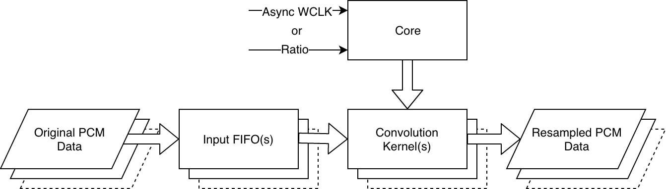
Application
In a typical application, the sample rate converter consists of three parts.
- One or more Input FIFO(s) that can hold enough samples for the convolution. Any number of input FIFOs may be connected to one core. Multiple variations are provided and can be used arbitrarily.
asrc_fifo_parallelaccepts pipelined parallel PCM input; channel count is 2CH_BITS (2 to 32 channels)asrc_fifo_tdm_4x8accepts serial TDM data with four strides, up to eight channels eachasrc_fifo_tdm_4x2accepts serial TDM data with four strides, two channels each
- The core itself (
asrc_core), which computes the right tap value for the convolution at the right time. The core also determines the ratio between input and output when set to asynchronous mode. One core is needed per direction. One core serves any amount of I/O channels. - One or more convolution kernels (
asrc_convolute). Each convolution kernel applies the actual resampling to the PCM data held in the respective input FIFO for up to 32 channels. The output is always random access parallel PCM and may be double buffered. Several examples are provided for converting the results to TDM, left-justified (LJ) serial format, or massive-parallel data.
For bidirectional resampling, the dedicated core asrc_core_bidir is provided. This actually instantiates two cores that share one set of coefficients as dual-ported ROM. In contrast to using two unidirectional cores in parallel, this saves LUT resources, and 8 to 12 kBytes of block RAM.
Block Diagram
Designing with the Core
It is recommended to use the sources directly by copying or sym-linking the contents of the rtl directory to your FPGA hdl sources directory. The provided examples demonstrate how to use the core with a variety of application scenarios.
If you prefer using pre-synthesized netlists, there are some helper scripts provided (ISE only). You need to select a target in the target.cfg file and run ./make_netlist.sh in the top directory of the package. A ngc file will be generated.
Asynchronous Mode
If the parameter MANUAL_RATIO is set to 0, the ratio between input and output word clocks is determined by the core. The internal moving average detector measures the time between two word clock events at 26 bits precision. The time constant is about one second. It also calculates the reciprocal that is needed to scale the output amplitude during downsampling. The direction signal reverses the average value with the reciprocal, hence allowing resampling to upstream.
| direction | Description |
|---|---|
| 1'b0 | Resample arbitrary incoming audio to the internal clock |
| 1'b1 | Resample internal audio to the foreign clock |
async_wclk_in may be connected directly to any asynchronous word clock source. The ASRC core handles re-registering internally.
Clock Domain Crossing
The asrc_core features the 8-bit output iodiv_out[7:0] , which is a copy of iodiv_r[30:23]. You may use this as an indicator in your application if you need to know at which ratio the resampler is currently working.
Synchronous Mode
If parameter MANUAL_RATIO is set to 1, the core does not derive the ratio from the input word clock. A valid ratio and its reciprocal must be given in 4.28 fixed point format to iodiv_manual and iodiv_r_manual. They may be changed arbitrarily at runtime without resetting the core.
async_wclk_in (the input pin for asynchronous word clock) is ignored in synchronous mode. The core just eats up the samples that are fed into the internal FIFO by triggering new_frame synchronously. Just like in asynchronous mode, there is no requirement on phase relationship between input and output word clock (other than being synchronous to the high frequency core clock).
iodiv_manual must represent the 4Q28 fixed point value of Fsin divided by Fsout and iodiv_r_manual, its reciprocal.
| Speed Mode In | Speed Mode Out | out_speedmode[1:0] | iodiv_manual[31:0] | iodiv_r_manual[31:0] |
|---|---|---|---|---|
| Single | Single | 2'd0 | 32'h1000_0000 | 32'h1000_0000 |
| Single | Double | 2'd1 | 32'h0800_0000 | 32'h2000_0000 |
| Single | Quad | 2'd2 | 32'h0400_0000 | 32'h4000_0000 |
| Double | Single | 2'd0 | 32'h2000_0000 | 32'h0800_0000 |
| Double | Double | 2'd1 | 32'h1000_0000 | 32'h1000_0000 |
| Double | Quad | 2'd2 | 32'h0800_0000 | 32'h2000_0000 |
| Quad | Single | 2'd0 | 32'h4000_0000 | 32'h0400_0000 |
| Quad | Double | 2'd1 | 32'h2000_0000 | 32'h0800_0000 |
| Quad | Quad | 2'd2 | 32'h1000_0000 | 32'h1000_0000 |
Reset Signal
The core is partly reset at active high of the reset input signal. You may tie this to your internal reset logic. This pin is optional. Tie to 1'b0 if not used.
In general, there is no lockup situation known to that the core would need a reset. If it gets wrong signals, it will output wrong values. If the fed signals become valid again, the core will resume with valid output. Use the asrc_health module to mute or re-route your outputs if invalid signals are unacceptable.
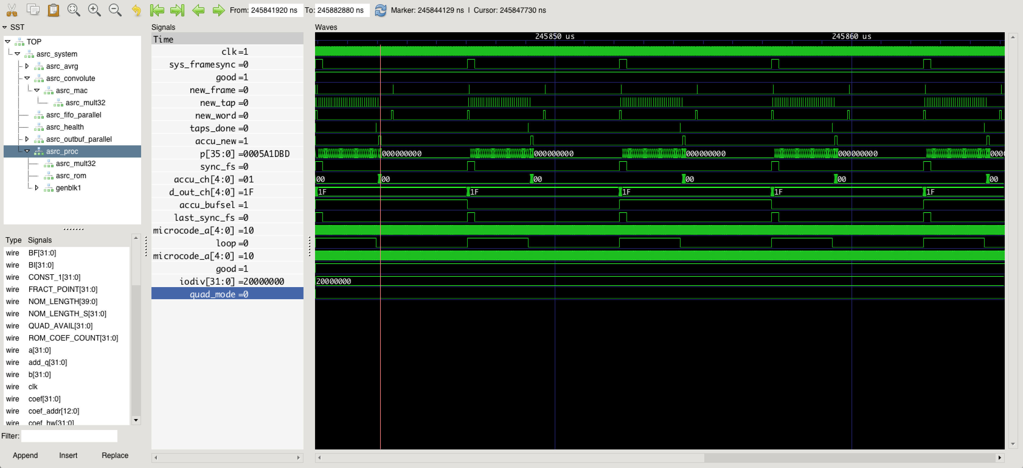
Health Module
The asrc_health module checks some states and the "good" output goes high if the internal FIFOs are not full or empty. It can be used to enable other circuity in the design, such as mute events.
Lock Signal
All reference modules expose a lock output. It goes high once the internal ratio detector has acquired a stable estimate of the input word clock frequency. Unlike the good output (which monitors FIFO fill level), lock reflects whether the ratio has converged to a usable value. In MANUAL_RATIO=1 mode or when force_manual is asserted, lock is asserted immediately after the core exits reset.
It is recommended to gate the en input of asrc_convolute with both good and lock to prevent output data from being produced before a valid ratio has been established. The provided reference modules use good && lock as the enable condition.
Force Manual Mode
The force_manual input allows overriding the asynchronous ratio detector at runtime. When high, it forces the core to use the values provided on iodiv_manual and iodiv_r_manual, even when the compile-time parameter MANUAL_RATIO is set to 0. This allows switching between asynchronous and manual-ratio operation at runtime without recompilation, for example for testing or fallback scenarios. When MANUAL_RATIO=1, force_manual is ignored by the core and may be tied to 1'b0.
External Coefficient Set
When the parameter EXT_FILTER is set to 1, the internal default coefficient ROM is bypassed and a user-supplied coefficient ROM is used instead. The core outputs the ROM read address on coef_ext_a[11:0] (12 bits, addressing up to 4096 entries). The user logic must supply the coefficient data on two separate inputs:
coef_ext_2048coefficients for the single and double speed set (2048 entries, accessed at addresses 0..2047)coef_ext_4096coefficients for the quad speed set (4096 entries, accessed at addresses 0..4095)
Both inputs are read in the same clock cycle as coef_ext_a is presented; the ROM must be synchronous with one clock cycle read latency.
The parameter LIN_ADDRESSING controls how the external coefficient ROM is interpreted:
LIN_ADDRESSING=0(default): The ROM is expected to contain only half the filter taps. The core internally mirrors the coefficients, assuming a symmetric (linear-phase) FIR filter. This halves the required ROM size.LIN_ADDRESSING=1: The ROM must contain the full filter (all taps in order). This allows non-symmetric filter designs, most notably minimum-phase FIR filters.
A minimum-phase FIR filter is a particularly valuable application. By concentrating all the impulse response energy at the start of the filter rather than distributing it symmetrically, pre-ringing is completely eliminated. A linear-phase FIR of length N has a constant group delay of exactly (N−1)/2 samples at all frequencies. The passband group delay of a minimum-phase FIR of the same length and stopband attenuation is typically approximately half that value (roughly (N−1)/4 samples near DC) though unlike linear phase this group delay is frequency-dependent, rising toward the band edge. For the ASRC this means the total latency reduces to essentially the internal FIFO fill position plus the input and output serialization overhead. The FIR filter contributes near-zero additional delay. Whether the non-linear phase response is acceptable depends on the application; for live sound and monitoring the latency reduction is generally far more significant than phase linearity. The minimum-phase filter is not included in the standard IP core license.
When EXT_FILTER=0 (default), all three signals and the LIN_ADDRESSING parameter are unused and may be left unconnected.
Sharing a Coefficient ROM Between Two Instances
Because the coef_ext_a/coef_ext_2048/coef_ext_4096 interface is a plain synchronous ROM port, any two ASRC instances with EXT_FILTER=1 can share a single coefficient ROM by instantiating it as a dual-ported RAM and connecting each port to one instance. The provided asrc_coef_2048 and asrc_coef_4096 modules already expose dual ports (addr_a/out_a and addr_b/out_b) for this purpose. Custom coefficient ROMs can follow the same pattern.
Both instances must use the same LIN_ADDRESSING value since they share the same ROM contents. This technique works with any module that has the coef_ext_* interface, including asrc_system_parallel_ramif_mp.
Deterministic Group Delay
In asynchronous mode (MANUAL_RATIO=0 and force_manual not asserted), the group delay is deterministic to within 1/16 of Fsin. This is an inherent property of the ratio detector and FIFO alignment algorithm and does not require any additional parameter setting.
This is useful in applications where precise, repeatable latency is required across resets or power cycles, such as live sound processing systems, tightly coupled multi-converter installations, or signal paths that must be aligned with another converter.
In manual ratio mode (MANUAL_RATIO=1 or force_manual asserted), the FIFO alignment carries a ±10 Fsout sample uncertainty (stable after lock, not jittering).
Core Clock
The core is designed and tested to be clocked at 122.288 MHz for 48/96/192k or at 112.896 MHz for 44.1/88.2/176.4k sample rates. It expects the local frame sync to happen every fclk / fsamplerate, which depends on the sample speed mode, as shown in the following table:
| Sample Speed | Core Clock Ticks per Output Frame |
|---|---|
| Single | 2560 |
| Double | 1280 |
| Quad | 640 |
The core triggers at rising edge of the target frame sync signal (out_framesync).
In synchronous mode (MANUAL_RATIO=1) any other core clock can be accepted by the core, as long the "ticks per output frame", as stated in the table above value, is attainable. For example if your system is clocked at 130 MHz, this will work perfectly fine.
Quad Mode
This core is designed to accept quad speed sample rates when the parameter QUAD_AVAIL is set to 1. Setting it to 0 will save 4096 bytes of occupied RAM and the highest acceptable samplerate will drop to about 113 kHz.
There is no hysteresis in changing internal modes when changing sample rate arbitrarily. Notably the edges between double and quad modes should be avoided. It is recommended to use the core within following sample rates:
Usable ranges are:
Fsin 30..113kHz and 115..200kHz.
The ratio between input and output samplerate must not be larger than 4.999.
Downsampling from 192 kHz
Downsampling from e.g. 192kHz to 48kHz is challenging because it would require 128 taps per Fsout which is beyond the maximum of possible taps in this design. It is common to skip the first half of the coefficients this case, effectively scaling it down to 64 taps. However, just skipping does not deliver enough amount of alias image rejection and this is not satisfying the standards of professional audio equipment. Hence, there is a second coefficient set available which is was optimized to 64 taps at quad downsampling rates.
Upsampling to 192 kHz
The maximum number of possible taps shrink down because the core algorithm needs 32 clock cycles to fetch and interpolate a polyphase tap. At 192 kHz, this would require a core clock of 245.76 MHz. Because this clock is not possible with today's budget FPGAs, this mode is implemented to use the second coefficient set that is available in half of the original size.
Determining Latency
The simulation has a single-shot peak detector implemented. The Fs time of the first positive peak of each input and output will be saved in a variable and the result is printed to the console when the simulation is done. This could also be implemented as zero-crossing detector but that technique suffers from false-positives when possible pre-ringing occurs, so peak detection is preferred.
Simulation done.

Measured latency: 10 fs_out samples
Provided Application Examples
Common Signals and Parameters
parameter QUAD_AVAIL
See Quad Mode.
parameter MANUAL_RATIO
See Synchronous Mode and Asynchronous Mode.
parameter CH_BITS
Sets the channel count per convolution kernel as a power of two: 2CH_BITS channels. Valid range is 1 to 5, giving 2 to 32 channels. Smaller values scale the convolution unit's memory usage down proportionally. CH_BITS=1 gives 2 channels at minimal resource cost. In modules that previously had a fixed 32-channel count, this parameter defaults to 5.
parameter EXT_FILTER
When set to 1, enables the external coefficient ROM interface. See the External Coefficient Set section above.
parameter LIN_ADDRESSING
Only relevant when EXT_FILTER=1. When 0 (default), the external coefficient ROM is assumed to contain half the filter taps and is internally mirrored (linear-phase symmetric filter assumed). When 1, the ROM must contain the full filter, enabling non-symmetric filters such as minimum-phase. See the External Coefficient Set section above.
output lock
High when the ratio detector has acquired a stable lock on the asynchronous word clock. See the Lock Signal section above.
input force_manual
When high, forces use of iodiv_manual/iodiv_r_manual regardless of the MANUAL_RATIO parameter. See the Force Manual Mode section above. Tie to 1'b0 if not used.
output [11:0] coef_ext_a, input [31:0] coef_ext_2048, input [31:0] coef_ext_4096
External coefficient ROM interface, active when EXT_FILTER=1. All three signals may be left unconnected when EXT_FILTER=0. See the External Coefficient Set section above.
For other individual signals, see the source files for further explanation of the individual ports.
Parallel pipelined Input and RAM-interfaced Output
Parallel input words are fed into the resampler at rising edge of new_word. After 2CH_BITS words have been fed, a new_frame pulse must follow to mark the end of frame.
The double buffered output can be read through the RAM interface with d_out_ch as address and d_out as data. The d_out_valid output indicates that the data at d_out is valid for the current address.
module asrc_system_parallel_ramif
#(
    parameter   CH_BITS         = 5,
    parameter   QUAD_AVAIL      = 1,
    parameter   MANUAL_RATIO    = 0,
    parameter   EXT_FILTER      = 0,
    parameter   LIN_ADDRESSING  = 0
)
(
    input           clk,
    input           reset,
    input           out_framesync,
    input   [1:0]   out_speedmode,
    input           direction,
    input           async_wclk_in,
    output          lock,

    output  [11:0]  coef_ext_a,
    input   [31:0]  coef_ext_2048,
    input   [31:0]  coef_ext_4096,

    input           force_manual,
    input   [31:0]  iodiv_manual,
    input   [31:0]  iodiv_r_manual,

    input           new_word,
    input           new_frame,
    input   [23:0]  d_in,

    input   [CH_BITS-1:0]
                    d_out_ch,
    output  [23:0]  d_out,
    output          d_out_valid,

    output          good
);
TDM, Unidirectional
Four lanes of eight channels, MSB first, with one-early frame sync. In the one-early convention the frame sync pulse rises one BCK period before the first data bit. The MSB of the first channel appears on the BCK edge immediately following the frame sync edge. This is the standard alignment used by many professional audio codecs (e.g. Cirrus Logic CS series) and gives the receiver a full BCK period to detect the frame boundary before the data stream begins. Also available as asrc_system_tdm_4x2, which handles four lanes of two channels.
Also available as asrc_system_tdm_4x2, which handles four lanes of two channels. It additionally accepts an optional tdm_in_lrck input for left-right clock alignment:
module asrc_system_tdm_4x8
#(
    parameter   QUAD_AVAIL      = 1,
    parameter   MANUAL_RATIO    = 0,
    parameter   EXT_FILTER      = 0,
    parameter   LIN_ADDRESSING  = 0
)
(
    input           clk,
    input           reset,
    input   [1:0]   out_speedmode,
    output          good,
    output          lock,

    output  [11:0]  coef_ext_a,
    input   [31:0]  coef_ext_2048,
    input   [31:0]  coef_ext_4096,

    // if MANUAL_RATIO = 1
    input   [31:0]  iodiv_manual,
    input   [31:0]  iodiv_r_manual,

    // if MANUAL_RATIO = 0
    input           force_manual,
    input           direction,
    input           async_wclk_in,

    input           tdm_in_bck,
    input           tdm_in_fs,
    input   [3:0]   tdm_in_d,

    input           tdm_out_bck,
    input           tdm_out_fs,
    output  [3:0]   tdm_out_d
);
Maximum BCK frequency for the TDM modules is 24.576 MHz.
TDM, Bidirectional
Same as unidirectional, but duplicated ports for additional resampling to upstream direction. This makes use of the bidirectional asrc_core_bidir, which will share the coefficient ROM between the two resamplers. Also available as asrc_system_tdm_4x16_bidir, which handles four lanes of sixteen channels each (64 channels total). This variant does not include the QUAD_AVAIL or EXT_FILTER parameters but the user can add them manually.
module asrc_system_tdm_4x8_bidir
#(
    parameter   QUAD_AVAIL   = 1,
    parameter   MANUAL_RATIO = 0
)
(
    input           clk,
    input           reset,
    input   [1:0]   out_speedmode,
    output          good,
    output          lock,

    // if MANUAL_RATIO = 1
    input   [31:0]  iodiv_manual,
    input   [31:0]  iodiv_r_manual,

    // if MANUAL_RATIO = 0
    input           force_manual,
    input           direction,
    input           async_wclk_in,

    input           tdm_in_bck,
    input           tdm_in_fs,
    input   [3:0]   tdm_in_d,

    input           tdm_out_bck,
    input           tdm_out_fs,
    output  [3:0]   tdm_out_d,

    // second resampler, other direction:

    input   [1:0]   out_speedmode_1,

    input           tdm_in_bck_1,
    input           tdm_in_fs_1,
    input   [3:0]   tdm_in_d_1,

    input           tdm_out_bck_1,
    input           tdm_out_fs_1,
    output  [3:0]   tdm_out_d_1,

    output          good_1
);
Massive Parallel
Exactly 32 parallel inputs and outputs (one group of 32 channels). The channel count is fixed to 32 in this module but is configurable via CH_BITS. An async_wclk_sync output provides a re-registered version of the asynchronous word clock synchronous to clk.
module asrc_system_parallel_32ch
#(
    parameter   CH_BITS         = 5,
    parameter   QUAD_AVAIL      = 1,
    parameter   MANUAL_RATIO    = 0,
    parameter   EXT_FILTER      = 0,
    parameter   LIN_ADDRESSING  = 0
)
(
    input               clk,
    input               reset,
    input   [1:0]       out_speedmode,
    output              good,
    output              lock,

    output  [11:0]      coef_ext_a,
    input   [31:0]      coef_ext_2048,
    input   [31:0]      coef_ext_4096,

    input               force_manual,
    input   [31:0]      iodiv_manual,
    input   [31:0]      iodiv_r_manual,
    input               async_wclk_in,
    output              async_wclk_sync,
    input               direction,

    input               wclk_in,
    input       [23:0]  pcm_in_1,
    input       [23:0]  pcm_in_2,
    input       [23:0]  pcm_in_3,
...
    input       [23:0]  pcm_in_31,
    input       [23:0]  pcm_in_32,

    input               wclk_out,
    output              pcm_out_valid,
    output reg  [23:0]  pcm_out_1,
    output reg  [23:0]  pcm_out_2,
    output reg  [23:0]  pcm_out_3,
...
    output reg  [23:0]  pcm_out_31,
    output reg  [23:0]  pcm_out_32
);
Multi-Group Parallel (RAM Interface)
asrc_system_parallel_ramif_mp (mp = multiply ports) scales to any multiple of 2CH_BITS channels by running MP parallel convolution kernels behind a single interface. The total channel count is MP × 2CH_BITS, up to 512 channels:
module asrc_system_parallel_ramif_mp
#(
    parameter   CH_BITS         = 5,
    parameter   MP              = 1,
    parameter   QUAD_AVAIL      = 1,
    parameter   MANUAL_RATIO    = 0,
    parameter   EXT_FILTER      = 0,
    parameter   LIN_ADDRESSING  = 0
)
(
    input           clk,
    input           reset,
    input           out_framesync,
    input   [1:0]   out_speedmode,
    input           direction,
    input           async_wclk_in,
    output          lock,

    output  [11:0]  coef_ext_a,
    input   [31:0]  coef_ext_2048,
    input   [31:0]  coef_ext_4096,

    input           force_manual,
    input   [31:0]  iodiv_manual,
    input   [31:0]  iodiv_r_manual,

    input           new_word,
    input           new_frame,
    input   [MP_W-1:0]
                    d_in_mp,
    input   [23:0]  d_in,

    input   [CH_W-1:0]
                    d_out_ch,
    output  [23:0]  d_out,
    output          d_out_valid,

    output          good
);
| MP | CH_BITS | Total channels |
|---|---|---|
| 2 | 5 | 64 |
| 3 | 5 | 96 |
| 4 | 5 | 128 |
| 16 | 5 | 512 |
Feeding input data
The signal d_in_mp[MP_W-1:0] selects which channel group (0 to MP−1) is currently being written. In practice, push 2CH_BITS samples into d_in with new_word for group 0, then increment d_in_mp and repeat for group 1, and so on through group MP−1, before issuing the new_frame pulse. Reading the output works the same as asrc_system_parallel_ramif: address all channels linearly via d_out_ch[CH_W-1:0].
All EXT_FILTER and coefficient-sharing options described above apply to this module as well.
Left-Justified (LJ) Output
Three example modules provide left-justified serial audio output. In I2S (Philips standard), the MSB of each sample appears on the second BCK rising edge after the LRCK transition — one BCK period of offset is part of the format definition. In Left-Justified, the MSB appears on the first BCK rising edge after the LRCK transition, with no offset. The two formats are otherwise identical in bit ordering and framing. Left-Justified is used by a number of professional and consumer codecs that do not implement the I2S one-cycle offset, and is compatible with several AES3-derived digital audio interfaces. These modules accept the same input interfaces as their TDM counterparts and are particularly suited for interfacing with such codecs.
asrc_system_lj_4x2 uses four strides of two channels each (8 channels total) with TDM input and LJ output. It accepts an optional tdm_in_lrck for left-right clock alignment on the input:
module asrc_system_lj_4x2
#(
    parameter   QUAD_AVAIL      = 1,
    parameter   MANUAL_RATIO    = 0,
    parameter   EXT_FILTER      = 0,
    parameter   LIN_ADDRESSING  = 0
)
(
    input           clk,
    input           reset,
    input   [1:0]   out_speedmode,
    output          good,
    output          lock,

    output  [11:0]  coef_ext_a,
    input   [31:0]  coef_ext_2048,
    input   [31:0]  coef_ext_4096,

    // if MANUAL_RATIO = 1
    input   [31:0]  iodiv_manual,
    input   [31:0]  iodiv_r_manual,

    // if MANUAL_RATIO = 0
    input           force_manual,
    input           direction,
    input           async_wclk_in,

    input           tdm_in_bck,
    input           tdm_in_fs,
    input           tdm_in_lrck,
    input   [3:0]   tdm_in_d,

    input           tdm_out_bck,
    input           tdm_out_fs,
    output  [3:0]   tdm_out_d
);
asrc_system_ramif_lj_4x2 accepts a pipelined parallel input (same as asrc_system_parallel_ramif) and outputs four LJ serial streams of two channels each:
module asrc_system_ramif_lj_4x2
#(
    parameter   QUAD_AVAIL      = 1,
    parameter   MANUAL_RATIO    = 0,
    parameter   EXT_FILTER      = 0,
    parameter   LIN_ADDRESSING  = 0

)
(
    input           clk,
    input           reset,
    input   [1:0]   out_speedmode,
    output          good,
    output          lock,

    output  [11:0]  coef_ext_a,
    input   [31:0]  coef_ext_2048,
    input   [31:0]  coef_ext_4096,

    // if MANUAL_RATIO = 1
    input   [31:0]  iodiv_manual,
    input   [31:0]  iodiv_r_manual,

    // if MANUAL_RATIO = 0
    input           force_manual,
    input           direction,
    input           async_wclk_in,

    input           new_word,
    input           new_frame,
    input   [23:0]  d_in,

    input           tdm_out_bck,
    input           tdm_out_fs,
    output  [3:0]   tdm_out_d
);
asrc_system_ramif_lj_1x2 is the single-stride variant with one LJ output stream carrying two channels:
module asrc_system_ramif_lj_1x2
#(
    parameter   QUAD_AVAIL      = 1,
    parameter   MANUAL_RATIO    = 0,
    parameter   EXT_FILTER      = 0,
    parameter   LIN_ADDRESSING  = 0

)
(
    input           clk,
    input           reset,
    input   [1:0]   out_speedmode,
    output          good,
    output          lock,

    output  [11:0]  coef_ext_a,
    input   [31:0]  coef_ext_2048,
    input   [31:0]  coef_ext_4096,

    // if MANUAL_RATIO = 1
    input   [31:0]  iodiv_manual,
    input   [31:0]  iodiv_r_manual,

    // if MANUAL_RATIO = 0
    input           force_manual,
    input           direction,
    input           async_wclk_in,

    input           new_word,
    input           new_frame,
    input   [23:0]  d_in,

    input           tdm_out_bck,
    input           tdm_out_fs,
    output  [0:0]   tdm_out_d
);
Simulation
Simulation is done using the high performance open source Verilog simulator Verilator, which effectively converts Verilog to C++. The output compiles to a native binary, which can be run on a PC.
Simulation presumes a Linux (or other Unix, e.g. Mac) command line terminal. On Windows, this may work using WSL (Windows Subsystem for Linux).
Prerequisites to run the Simulation
Find dependencies and installation instructions of the Verilator simulation suite on this web site. It is recommended to build from Git.
On Debian-flavoured systems, the installation of Verilator including dependencies is simple:
sudo apt-get install verilator
Running a Simulation
The system top module, written in C++, generates a stimulus. This is one of static sine tone, swept sine tone or Dirac impulse and it outputs a mono WAV file with the simulated result. Static sine tone is used for THD+N calculation. Swept sine can be used to show aliasing images using sndfile-spectrogram (which is part of libsndfile sndfile-tools). The Dirac stimulus will create an impulse response that can be used to inspect the frequency response by using deconvolution.
Verilator uses a much faster simulation technique than classical simulators, such as Icarus Verilog. You can expect to simulate five seconds of signal in ten to thirty seconds on a decent machine. Classic simulators would need several hours or even days for the same task.
For signal inspection using GTK Wave or the like, Verilator can output simulation data in VCD file format. You need to set WRITE_TRACE to 1 at the top of the corresponding C++ file.
Example session to observe the signals using GTK Wave:
Example: asrc_system_parallel_32ch
This example takes the synthesizable asrc_system_parallel_32ch.v found in the examples directory. It creates a signal and writes the resamples PCM to standard WAV files. The simulation stimulus is created in asrc_system_parallel_32ch.cpp. The shell script asrc_system_parallel_32ch.sh helps with building and running the simulation.
Run the simulation on the console with
./asrc_system_parallel_32ch.sh <what> <inrate> <outrate>
<What> is: 0=IR (Dirac) 1=sine 2=sweep
The example outputs 32 WAV files, following a special naming convention. Watch the console output.
$# ./asrc_system_parallel_32ch.sh 2 96003 48000
... (some compiler output)

Simulation started using SIM_WHAT=sweep FS_IN=96003 FS_OUT=48000
fs_cnt=12000 fs_cnt_in=24000.750005 iodiv=20004189 iodiv_r=7ffef9d sr=96002.99996
	out_data_count=11999 quad_mode=0 good=1
fs_cnt=24000 fs_cnt_in=48001.500821 iodiv=20004189 iodiv_r=7ffef9d sr=96002.99996
	out_data_count=23999 quad_mode=0 good=1
...

Simulation done.
WAV file 'asrc_sim-96003-48000-ch_1-sweep.wav' written.
Spectrogram 'asrc_sim-96003-48000-ch_1-sweep.wav.png' written.
WAV file 'asrc_sim-96003-48000-ch_2-sweep.wav' written.
Spectrogram 'asrc_sim-96003-48000-ch_2-sweep.wav.png' written.
....
Simulation output file name convention: asrc_sim-<Fs in>-<Fs out>-<what>.wav
Inspect the WAV files with the tools of your trust.
Performance
THD+N
Measured THD+N @ 0 dBFS 1 kHz sine BW 22Hz-22kHz for exemplary.
Fsout and Fsin are completely separate, asynchronous systems
| Fsout Hz | Fsin Hz | THD+N dB |
|---|---|---|
| 96000 | 32000 | -143.7 |
| 96000 | 44100 | -139.9 |
| 96000 | 48000 | -145.5 |
| 96000 | 88200 | -139.2 |
| 96000 | 96000 | -144.7 |
| 48000 | 32000 | -138.5 |
| 48000 | 44100 | -137.1 |
| 48000 | 48000 | -144.6 |
| 48000 | 88200 | -140.2 |
| 48000 | 96000 | -144.8 |
| 48000 | 192000 | -145.7 |
| 48003 | 192000 | -144.5 |
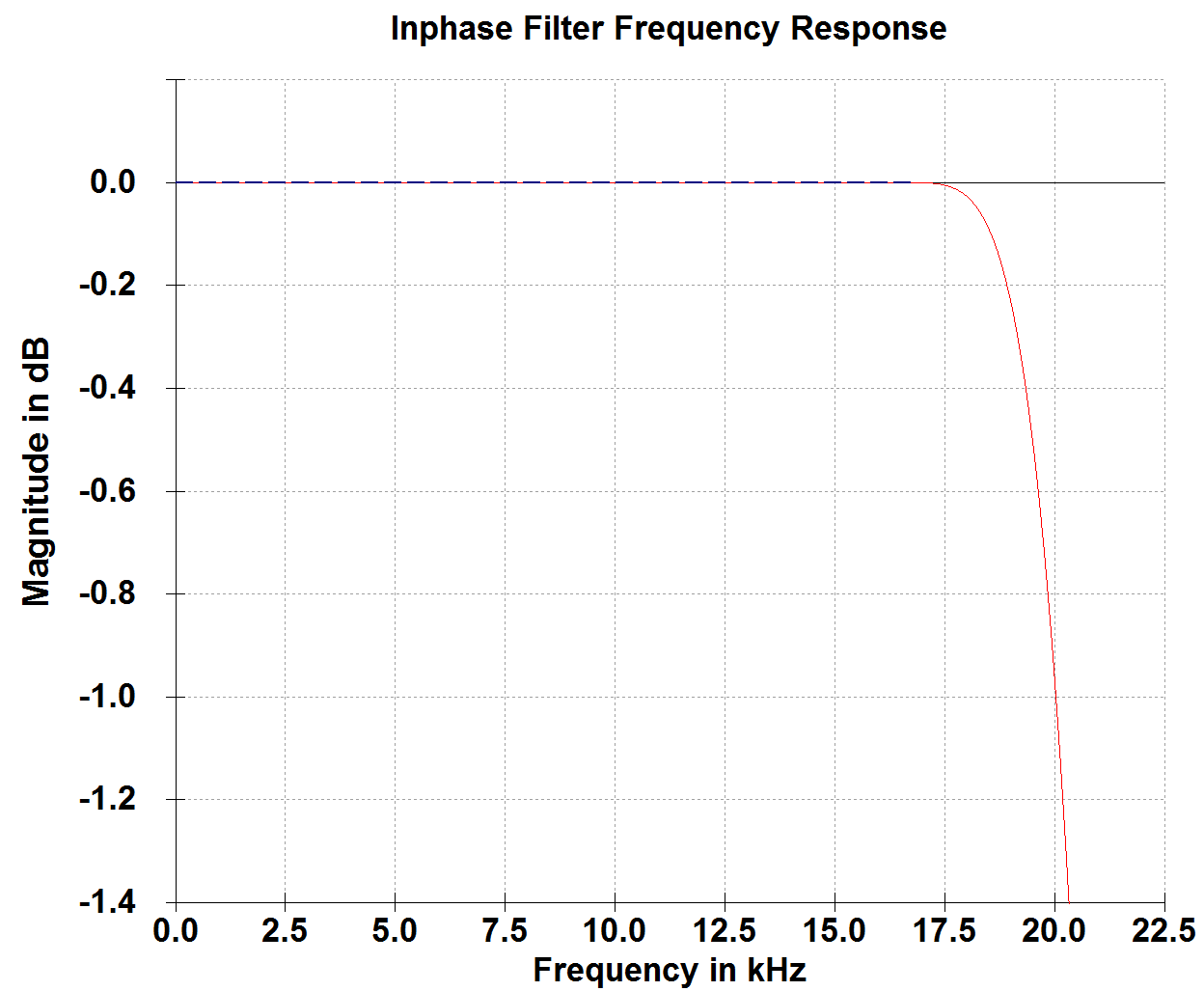
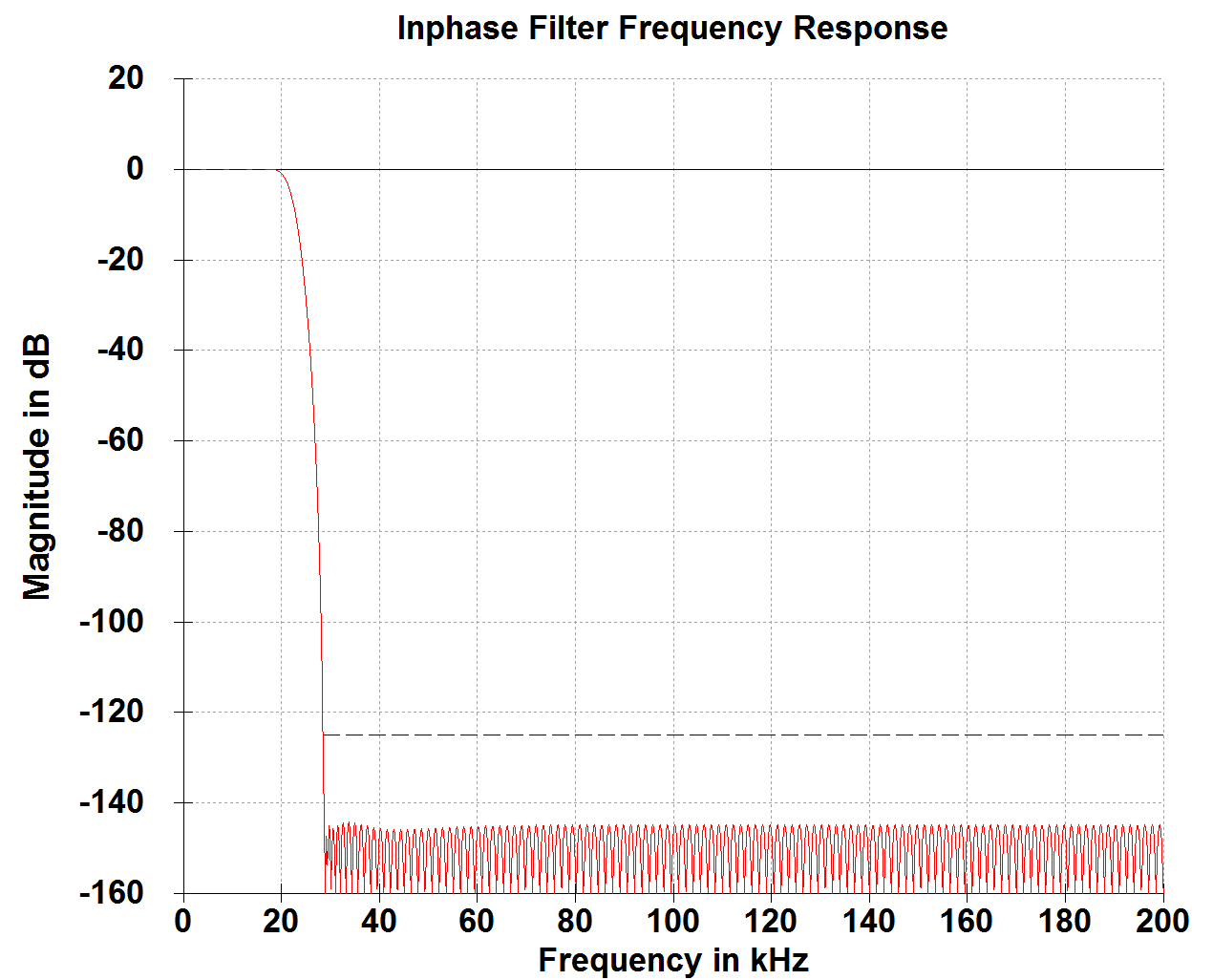
Frequency Response
Typical frequency response is +/-0dB at 0-18kHz and +0/-1.0dB at 0-20kHz.
Gain is about -0.05dB. This has not been set to 0 dB because of potential rounding errors of the scaling gain when upsampling. The scaling gain is calculated by the reciprocal of the given iodiv value (which is Fsin divided by Fsout).
The response is optimized to get shortest group delay as possible. Having -1 dB at 20 kHz might be considered a weakness by datasheet purists but this decision was the key to reach shortest group delay while maintaining excellent aliasing rejection within the audio band.
Illustrated frequency response represents double to single speed conversion with ratio=0.5. The actual frequency response may vary over different ratios.
Group Delay
The phase response is linear. Hence, regardless of the frequency, the absolute latency always corresponds to the group delay.
| Fsin | Fsout | 1/Fsout | Time (rounded) |
|---|---|---|---|
| 48000 | 48000 | 19 | 396 µs |
| 96000 | 48000 | 18 | 375 µs |
| 192000 | 48000 | 11 | 229 µs |
| 48000 | 96000 | 33 | 344 µs |
| 96000 | 96000 | 18 | 188 µs |
| 192000 | 96000 | 11 | 115 µs |
| 48000 | 192000 | 35 | 182 µs |
| 96000 | 192000 | 19 | 99 µs |
| 192000 | 192000 | 10 | 52 µs |
The delay is subject to change by +- 1 sample (Fsout) because of some residual uncertain FIFO alignment owed to asynchronous systems (but it won't jitter).
The latency can be further reduced by 2-3 samples when lowering FIFO_COUNT_MIN in asrc_convolute.v if limiting the maximum ratio is acceptable.
Resource Utilization
On the example of using TDM I/O, one direction, QUAD_AVAIL set to 0.
Device vs. Maximum Channel Count
| Series | Device | Channels |
|---|---|---|
| Spartan 6 | XC6SLX4 | 32 |
| Spartan 6 | XC6SLX9 | 96 |
| Spartan 6 | XC6SLX16 | 224 |
| Spartan 6 | XC6SLX25 | 256 |
| Artix 7 | XC7A35T | >1024 |
Channel Count vs. Occupied Slices
| Series | Channels | Occupied Slices |
|---|---|---|
| Spartan 6 | 32 | 430 |
| Spartan 6 | 64 | 510 |
For reference, XC6SLX9 has 1430 Slices.
Evaluation of the Core using Digilent Arty
An evaluation license with hardware timeout is available for this core in form of a ready-made bitstream. The sources are included with the purchased license.
See instructions below.
Connecting the Core
Arty Pmod Pinout
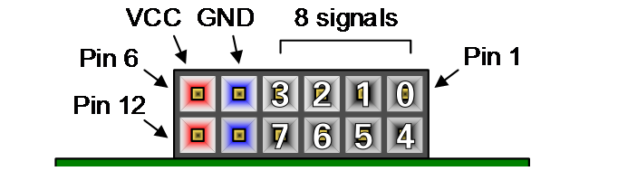
Bit numbers depicted in white digits.
FPGA Pinout Map
| Pin | Bit | Pmod JA | Pmod JB | Pmod JC | Pmod JD |
|---|---|---|---|---|---|
| Pin 1 | 0 | G13 | E15 | U12 | D4 |
| Pin 2 | 1 | B11 | E16 | V12 | D3 |
| Pin 3 | 2 | A11 | D15 | V10 | F4 |
| Pin 4 | 3 | D12 | C15 | V11 | F3 |
| Pin 7 | 4 | D13 | J17 | U14 | E2 |
| Pin 8 | 5 | B18 | J18 | V14 | D2 |
| Pin 9 | 6 | A18 | K15 | T13 | H2 |
| Pin 10 | 7 | K16 | J15 | U13 | G2 |
Actual Connections
Alls signals are LVCMOS 3.3V.
Direction (input or output) as seen from board perspective.
| Pmod, Bit | Direction | Signal |
|---|---|---|
| JA0 | Input | Input TDM Data Stride A (Channel 0..7 or 0..1) |
| JA1 | Input | Input TDM Data Stride B (Channel 8..15 or 2..3) |
| JA2 | Input | Input TDM Data Stride C (Channel 16..23 or 4..5) |
| JA3 | Input | Input TDM Data Stride D (Channel 24..31 or 6..7) |
| JA6 | Input | TDM Bitclock for inputs |
| JA7 | Input | TDM FS for inputs |
| JC0 | Output | "fifo good" |
| JC2 | Output | Master Clock Derived divided by 512 |
| JC3 | Input | Asynchronous FS input (e.g. tie to JA7 or JD7 depending on the "direction" switch) |
| JD0 | Output | Resampled TDM Data Stride A (Channel 0..7 or 0..1) |
| JD1 | Output | Resampled TDM Data Stride B (Channel 8..15 or 2..3) |
| JD2 | Output | Resampled TDM Data Stride C (Channel 16..23 or 4..5) |
| JD3 | Output | Resampled TDM Data Stride D (Channel 24..31 or 6..7) |
| JD4 | Input | 24.576 MHz Master Clock 50% duty (fed to PLL for internal high speed clock) |
| JD6 | Input | TDM Bitclock for outputs |
| JD7 | Input | TDM FS for outputs |
Switches
| Indicator | Description |
|---|---|
| SW0 | out_speedmode[0] |
| SW1 | out_speedmode[1] |
| SW2 | Direction |
| SW3 | LD4 on/off |
Status Indicators
| Indicator | Description |
|---|---|
| LD4 | on state of SW3, to verify switch knob direction |
| LD6 | "fifo good" |
| LD7 | 7 Hz blink |
Signal Constraints
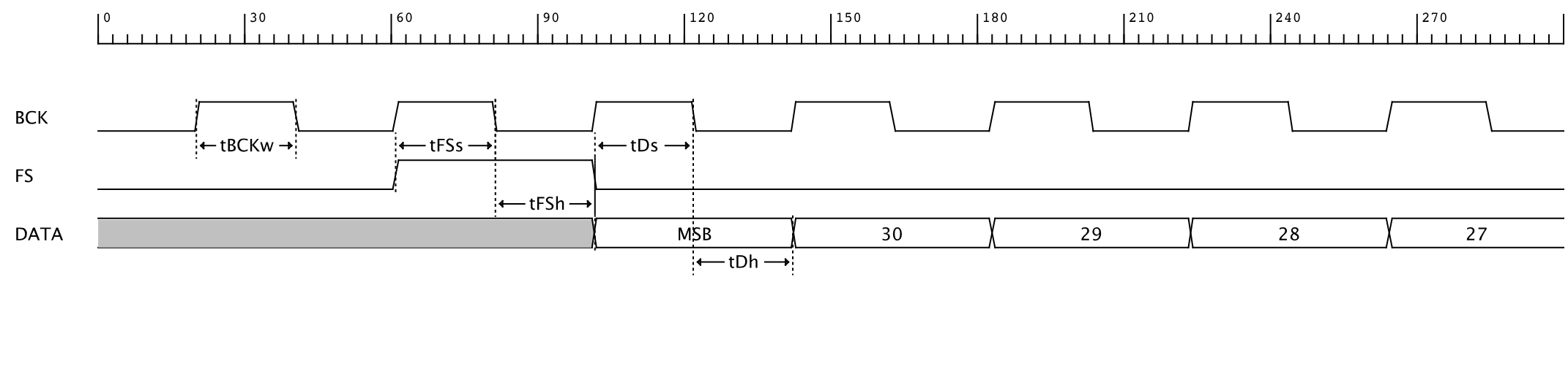
| Name | Min |
|---|---|
| tBCKw | 20 ns |
| tFSs | 16 ns |
| tFSh | 16 ns |
| tDs | 16 ns |
| tDh | 16 ns |
When using the 32-channel example, you may run into signal integrity issues because of the high bit clock frequency. Keep cables short and groundings low-z.
Binaries
Pre-made binaries for evaluation are included in the src/target/Arty_xxx/build directory.
| Target | Description |
|---|---|
| Arty_4x8 | Four TDM I/O, eight channels each |
| Arty_4x2 | Four TDM I/O, two channels each |
How to flash the demo binary to the board
- Connect the Micro-USB of Arty board to your host computer
- Run or flash the file .bin-file either using openFPGAloader or if you prefer full-stack double clicking, use the guide linked here
- Press the PROG button
- The DONE led turns on after a second
- LD7 flashes at a frequency of approx. 7 Hz if your input clock is valid
- The IP is up and running
When using the 32-channel example, quad speed mode output is not working because this would violate the maximum bit clock frequency of 24.576 MHz.
Appendix
Definition of Speed Modes
This document makes use of the term "speed" as a reference to original 44.1k or 48k sample rates. Following table clarifies the relationship.
| Sample Rate | Resulting "Speed" |
|---|---|
| 30000 to 56500 | Single |
| 57000 to 113000 | Double |
| 114000 to 230000 | Quad |
The two standard core clock frequencies derive from the two professional audio sample rate families. 122.88 MHz = 48000 × 2560 (the 48 kHz family: 48/96/192 kHz), and 112.896 MHz = 44100 × 2560 (the 44.1 kHz family: 44.1/88.2/176.4 kHz).
Document version: 110 / Jun 17, 2026 11:25
Download this document as PDF